Capture CISPCB Editor
From schematic to board: the Design Entry CIS → Allegro X PCB Editor flow
How to prepare libraries, generate the netlist and move the design from Capture CIS to PCB Editor without footprint errors.
Picture opening the box from the fab and watching your board power up the first time — no rework, no surprises at inspection. Twenty-five years designing where failure was not an option: defense and aerospace systems and, today, DDR4/DDR5 memory test modules. Here, that experience becomes a method you can apply on your very next project.
Every article comes from decisions made on real projects — and you notice the difference when the board comes back from the fab.
Two decades in defense and aerospace systems, with IPC Class 2 and 3 criteria, HDI and wraparound RF antennas. Rigor that becomes habit.
DDR4/DDR5 modules and memory test boards: stackup, controlled impedance, differential pairs and delay matching — signal integrity from the first trace.
Electronics engineer and lawyer (OAB/SP, Brazil): intellectual property, supplier contracts and compliance handled with the same precision as the layout.
“When the engineering is precise and the contract is clear, the project finds the shortest path from schematic to production.”
How to prepare libraries, generate the netlist and move the design from Capture CIS to PCB Editor without footprint errors.
How to build the layer stackup, calculate impedance in the cross-section editor and align everything with your fabricator.
Structure constraint sets, net classes and regions so that DRC works for you from the very first trace.
How to name, draw and validate footprints in Allegro X with IPC-7351 rules and the Padstack Editor.
Understand both approaches, when the classic formula is enough, and how to use our calculator.
A complete checklist to generate a fabrication and assembly package the fabricator understands the first time.
The articles follow the real order of work and point to the Allegro X menus and the applicable IPC standard for each decision.
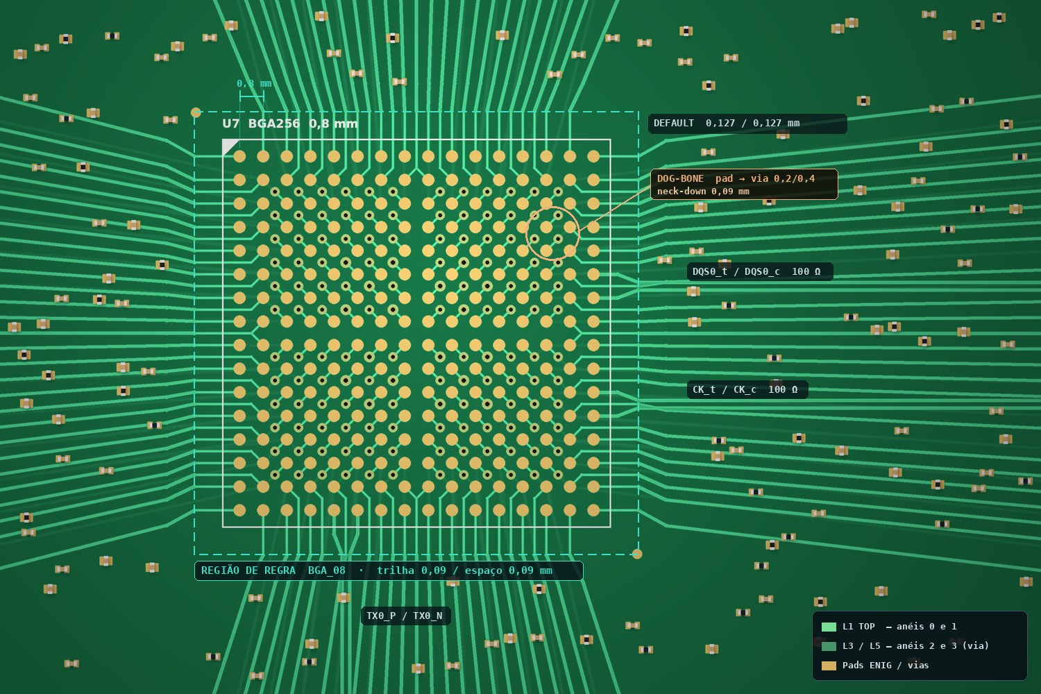
Shortcuts, menus and rules of thumb for everyday Allegro X work.
Display > Status shows DRCs, unrouted nets and out-of-date shapes in one place. Open it before generating any output.
Tools > Database Check with DRC and shape updates fixes database inconsistencies before the final review.
Shape > Global Dynamic Parameters adjusts thermal reliefs and void clearances of all dynamic shapes at once.
After fixing a footprint in the library, use Place > Update Symbols to bring the new version into the board.
Setup > Design Parameters holds units, decimal accuracy, grids and display. Set them in the company template.
Before the netlist, generate a BOM including the PCB Footprint property and filter blanks: the fastest way to find symbols without a footprint.
Enter current, temperature rise and copper thickness to get the minimum width in mm and mil. Includes a mil ↔ mm converter.
Open toolsA section dedicated to legal topics related to hardware and technology development.